Co-packaged optics places photonic and electronic chips in close contact, motivating the need for photonic components to be designed together with their surroundings and over larger design spaces. One solution to this is to frame the design problem as gradient-based optimization, also referred to as inverse design. However, this approach has historically found sparse use as it produces results that are hard to interpret and fabricate and are sensitive to fabrication variation. We describe a design flow that combines a global search for a starting design, adjoint shape optimization of every grating tooth in one or two layers, and an objective evaluated across the operating band and across samples of fabrication variation. In a design example, the flow raises the coupling efficiency of a dual-layer grating coupler from 34 % for the best uniform grating to 57 %. Recently, TSMC measured inverse-designed dual-layer couplers across a wafer, with a 1-dB bandwidth of 62 nm against 24 nm for its silicon coupler, at 1.16 dB against 0.98 dB loss [1]. These results indicate that automated design can now be considered a viable approach to producing components for industrial photonic processes.
Why design gets harder in co-packaged optics
Conversion between optical and electronic signals, such as in the links between switches in a data center, typically happens through well-separated interfaces. Most links still use pluggable transceivers at the switch front panel, which reach the switch chip through long, lossy electrical paths across the circuit board [2]. Co-packaged optics is a new trend that moves the optical engines into the same package as the switch or processor chip, shortening the electrical path to millimeters. As a result, the power required per bit drops significantly [2], and much higher bandwidth can be achieved [3]. However, it also introduces a challenge in design, because the pieces are now coupled (Fig. 1).
For example, the optical response of a component may now depend on the heat from the switch chip and the electronic chip above it, the metal and fill layers around it, and the high optical power delivered by external lasers [3, 4]. A component designed in isolation can perform differently in production. To model this system, we therefore need simulations that include the package stack, and design methods that tailor each component to it rather than picking from a library of standard components.
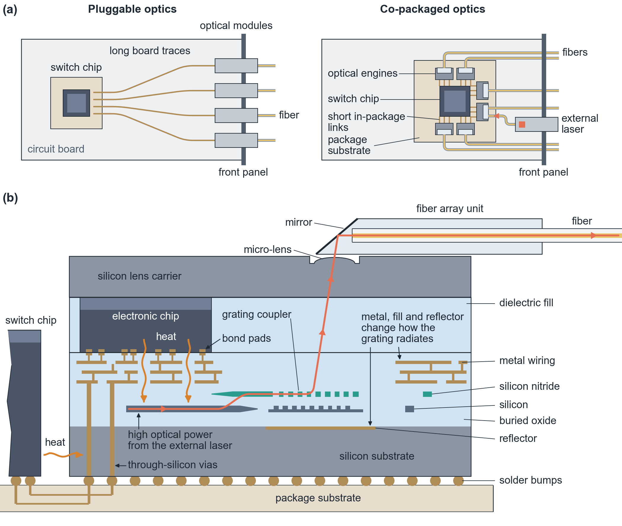
Figure 1. (a) Pluggable optics, with optical modules at the front panel, and co-packaged optics, with optical engines next to the switch chip in one package and an external laser source. (b) Cross-section of a co-packaged optical engine (not to scale). Light leaves the waveguide through the grating coupler and passes through the fill, a micro-lens and a mirror into the fiber. Heat, electrical connections and nearby layers all act on that path.
Grating couplers
One of the most important functions in any photonic system, including co-packaged optics, is coupling light from an optical fiber to a waveguide on the chip through free space. While edge couplers are a common choice for co-packaged optics [3], some platforms use grating couplers instead. Grating couplers accomplish this with a periodic set of teeth that scatters the guided light upward into the fiber. This configuration allows fibers to align vertically onto the chip, which can be advantageous for some setups. Because light must enter and leave the chip through such a fiber-to-chip interface, its loss directly limits the overall loss and bandwidth of the device, and it is therefore important to optimize its performance.
A common strategy to improve the coupler is to add a second grating layer, which gives the design more degrees of freedom (Fig. 2). Silicon nitride is an attractive choice for that layer: its lower refractive index widens the optical bandwidth, and it does not suffer the two-photon absorption that limits silicon at high optical power. Its low index contrast also makes strong upward emission hard on its own, which is one reason to pair it with silicon [5]. We describe measured dual-layer couplers of this kind below [1]. As the second layer doubles the number of teeth, the coupler is difficult to design with common heuristics and is therefore a good candidate for automated inverse design.
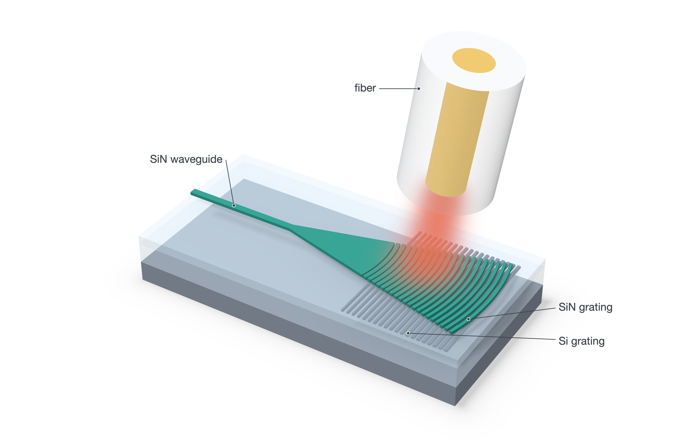
Figure 2. A dual-layer grating coupler. Light in the silicon nitride waveguide (left) is scattered upward by two gratings, one in silicon nitride and one in silicon, into a single-mode fiber tilted a few degrees from vertical.
Inverse design using shape optimization
In the inverse design approach, we write the design goal as a single number that we compute through simulation, such as the power coupled into the fiber, and consider the geometric features as free parameters in an optimization. We add constraints, such as a minimum feature size, and let an optimizer improve all parameters at once. With so many parameters, it is more efficient to compute the gradient of our design goal with respect to all of the parameters and update them iteratively until converging on a good result. In Tidy3D, this capability is built into the finite-difference time-domain (FDTD) solver through the adjoint method, which gives this gradient in just two simulations, no matter the number of parameters. Interestingly, this is analogous to the technique used to train neural networks, which similarly have enormous numbers of weight parameters that are optimized to minimize a loss function.
The most common form of inverse design in photonics is topology optimization, where we consider our device as parameterized by a grid of pixels that can be independently updated, similar to an image. For a 6.4 µm square region at 10 nm resolution, this contains 410,000 free parameters, so gradient-based optimization is the only realistic choice. Topology optimization can converge on designs that work well in simulation, but the results are hard to interpret and contain features too small to fabricate unless length-scale constraints are added [6]. Nevertheless, foundry-constrained methods [6, 7] and multi-layer grating couplers measured in a commercial process [8] show progress, and dual-layer silicon nitride and silicon grating couplers designed by global optimization under foundry rules have been measured across a 200 mm wafer [12].
Shape optimization takes a different route, which turns out to be more practical for many engineering problems (Fig. 3). We may compute the gradient with respect to the position of each boundary in our simulation using a variation of the same adjoint method [9]. This allows us to keep the parameters tied to real geometric quantities, for example the width and position of each tooth or the control points of a spline. Therefore, our final design stays interpretable, the design rules become simple bounds, and the number of parameters can be small enough for global methods such as BONNI [10] or large enough for gradient descent.
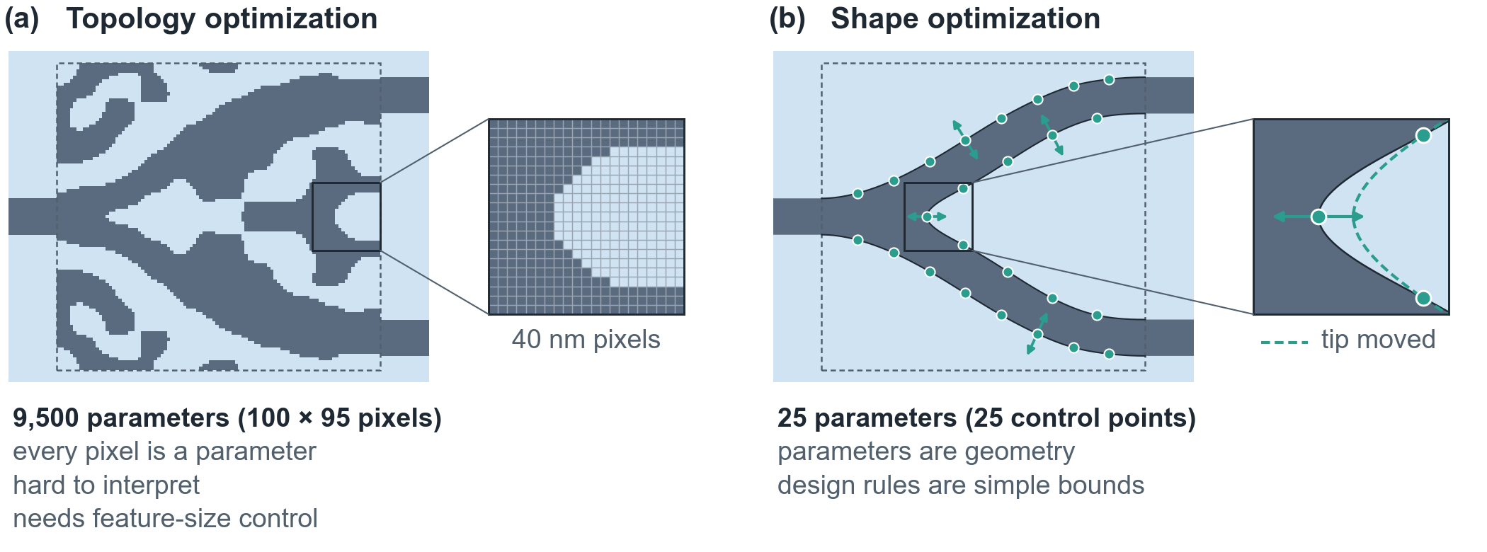
Figure 3. The same 1x2 power splitter parameterized two ways; the dashed box is the 4.0 µm by 3.8 µm design region. (a) Topology optimization: a design from our 2D adjoint optimization in which each of the 9,500 pixels (40 nm) is a parameter; the inset shows the pixel grid. (b) Shape optimization: the boundary is a spline through 25 control points, each moving along the boundary normal; the inset shows the boundary after the tip point moves.
Method
For grating coupler problems using shape optimization, we use a workflow that has three stages (Fig. 4). First, we pick a starting design: an existing grating, or the result of a global search over a few parameters. In our seminar notebooks, we used Bayesian optimization to search the tooth widths, gaps and layer offset [11]. Next, gradient-based refinement is used to adjust the width and gap of every tooth in each layer. Finally, at each step, the design rules are checked, and any tooth or gap that falls below the minimum line or gap is clipped.
To account for manufacturability, we adjust the objective function over the simulation outputs to tune the desired performance of the device under various conditions. For example, we evaluate coupling at several wavelengths across the band and across several samples of fabrication variation (such as tooth width, layer thickness and the alignment between layers). We combine these values with a smooth minimum, so the optimizer works on the worst case rather than the average. Each fabrication sample still only requires one broadband forward simulation and one adjoint simulation, which together give the gradient of this objective with respect to every parameter.
We run the flow in Tidy3D, which can compute adjoint gradients with respect to geometric parameters using its automatic differentiation support for autograd, JAX, and PyTorch. A public version of this process is in our inverse design seminar notebooks [11].
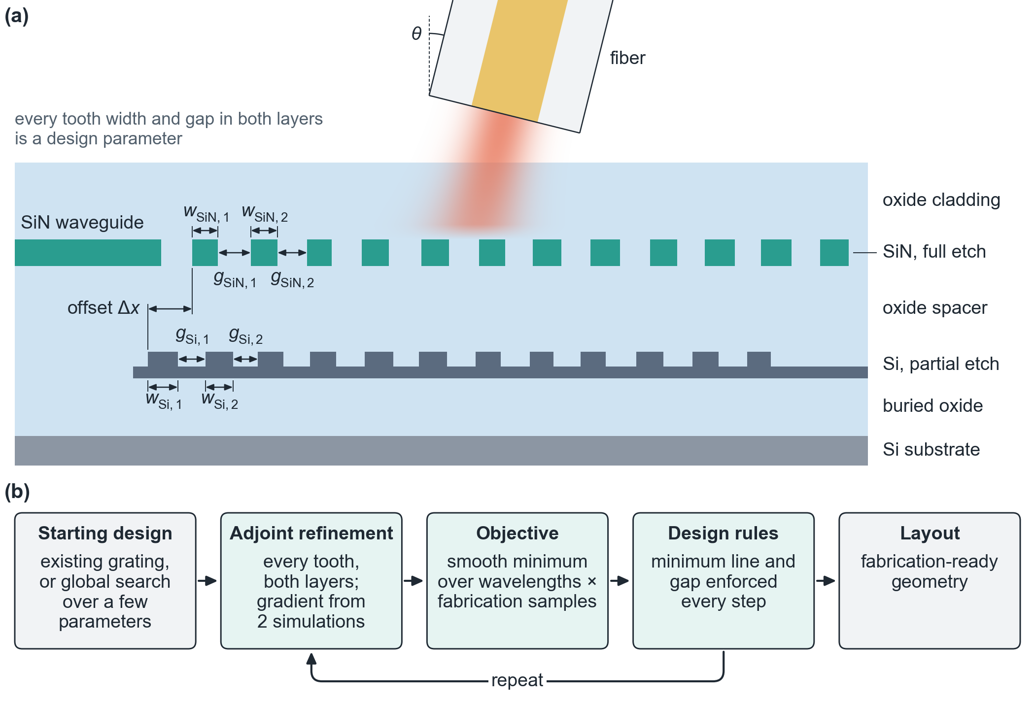
Figure 4. (a) Design parameters: the width and gap of every tooth in both layers, and the offset between the gratings. (b) The design flow: a starting design, from an existing grating or a global search, then adjoint refinement against an objective over wavelengths and fabrication samples, with design rules enforced at every step.
Design example: a dual-layer grating coupler
To show the workflow end to end, we design a dual-layer grating coupler in simulation on a generic stack from our public seminar notebooks [11], with 15 teeth in each of a silicon and a silicon nitride layer and a target wavelength of 1.55 µm.
A uniform grating with a 50 % duty cycle couples almost no light. A Bayesian search over five parameters of a uniform grating raises the coupling efficiency to 34 % (Fig. 5a). Adjoint refinement of every tooth’s width and gap, about 60 parameters, then raises it to 57 %.
The refined design is tuned to the nominal geometry, so fabrication variation costs it about 0.1 dB on average, and 0.4 dB or more in the worst 10 % of cases (Fig. 5b). Adding fabrication variation to the objective recovers part of that loss.
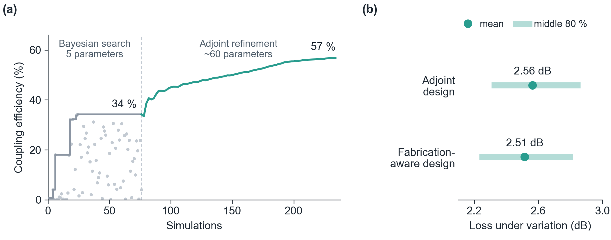
Figure 5. Design example for a dual-layer grating coupler at 1.55 µm, from our public seminar notebooks [11]. (a) Coupling efficiency over the design run: every Bayesian-search evaluation of a uniform grating (dots) with the best so far (gray line), then adjoint refinement of every tooth (teal), at two simulations per iteration. (b) Loss under 100 Monte Carlo samples of fabrication variation, with standard deviations of 25 nm in layer alignment, 20 nm in spacer thickness and 10 nm in silicon tooth width, for the adjoint design and for a design re-optimized over ±20 nm etch corners: the mean and the middle 80 % of samples.
Measured dual-layer couplers
In an OFC 2026 paper we co-authored with TSMC [1], TSMC fabricated dual-layer silicon and silicon nitride grating couplers designed by a particle-swarm search followed by adjoint shape optimization, and measured them across 29 dies of one wafer. They reached a 1-dB bandwidth of 62 nm, against 24 nm for the platform’s silicon grating coupler, at an insertion loss of 1.16 dB against 0.98 dB.
The paper also tested how the couplers handle heat and high optical power, two stresses that co-packaging adds. Between 25 and 105 °C, the dual-layer coupler’s loss changed by at most 0.13 dB, against up to 1 dB for silicon. Its loopback test structure showed no absorption loss up to 24 dBm, the instrument limit, while silicon began to absorb near 15 dBm.
Takeaway and next steps
Shape-based inverse design produces grating couplers that are interpretable and meet foundry design rules by construction. On a dual-layer coupler, the workflow in this post raised coupling from 34 % for the best uniform grating to 57 % and quantified how much fabrication variation costs the design. The measured couplers in [1] have more than twice the bandwidth of the platform’s silicon coupler, at 0.18 dB more loss. A next step is to measure fabrication-aware designs across wafers to quantify the gain in yield.
The techniques are available through our simulation platform and public notebooks [11]. As the method is general, it applies equally to any photonic device design process, within co-packaged optics or outside it. Furthermore, it scales naturally from single-component design to full-chip design, where AI agents can run the same simulate-and-optimize loop autonomously against a system-level objective [13].
Acknowledgments
We thank Greg Roberts, Prashanta Kharel and Momchil Minkov for comments on the draft.
References
- N. N. Shi et al., “Adjoint-optimized Dual-Layer Grating Couplers for Low-Loss, High-Bandwidth Optical Interconnects,” OFC 2026, paper Tu2J.2.
- A. Seyedi, “Scaling AI Factories with Co-Packaged Optics for Better Power Efficiency,” NVIDIA Technical Blog (August 2025).
- M. Tan et al., “Co-packaged optics (CPO): status, challenges, and solutions,” Front. Optoelectron. 16, 1 (2023).
- OIF, “External Laser Small Form Factor Pluggable (ELSFP) Implementation Agreement,” OIF-ELSFP-02.0 (2025).
- R. Marchetti, C. Lacava, L. Carroll, K. Gradkowski, and P. Minzioni, “Coupling strategies for silicon photonics integrated chips,” Photon. Res. 7, 201 (2019).
- M. F. Schubert, A. K. C. Cheung, I. A. D. Williamson, A. Spyra, and D. H. Alexander, “Inverse design of photonic devices with strict foundry fabrication constraints,” ACS Photonics 9, 2327 (2022).
- A. Y. Piggott et al., “Inverse-designed photonics for semiconductor foundries,” ACS Photonics 7, 569 (2020).
- A. M. Hammond, J. B. Slaby, M. J. Probst, and S. E. Ralph, “Multi-layer inverse design of vertical grating couplers for high-density, commercial foundry interconnects,” Opt. Express 30, 31058 (2022).
- C. M. Lalau-Keraly, S. Bhargava, O. D. Miller, and E. Yablonovitch, “Adjoint shape optimization applied to electromagnetic design,” Opt. Express 21, 21693 (2013).
- Y. Mahlau, Y. Augenstein, T. W. Hughes, M. Lindauer, and B. Rosenhahn, “BONNI: Gradient-informed Bayesian and interior point optimization for efficient inverse design in nanophotonics,” arXiv:2602.18148 (2026).
- Flexcompute, “Fabrication-aware inverse design,” Tidy3D seminar notebooks (October 2025), github.com/flexcompute/tidy3d-notebooks/tree/develop/2025-10-09-invdes-seminar.
- J. C. C. Mak, Q. Wilmart, S. Olivier, S. Menezo, and J. K. S. Poon, “Silicon nitride-on-silicon bi-layer grating couplers designed by a global optimization method,” Opt. Express 26(10), 13656 (2018).
- P. Kharel, A. Khavasi, X. Chen, and T. W. Hughes, “Autonomous agentic design for photonics,” arXiv:2606.00915 (2026).