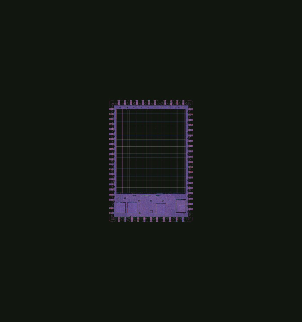
The 38M-shape Efabless Caravel electronic die on sky130, loaded in the PhotonForge LiveViewer.
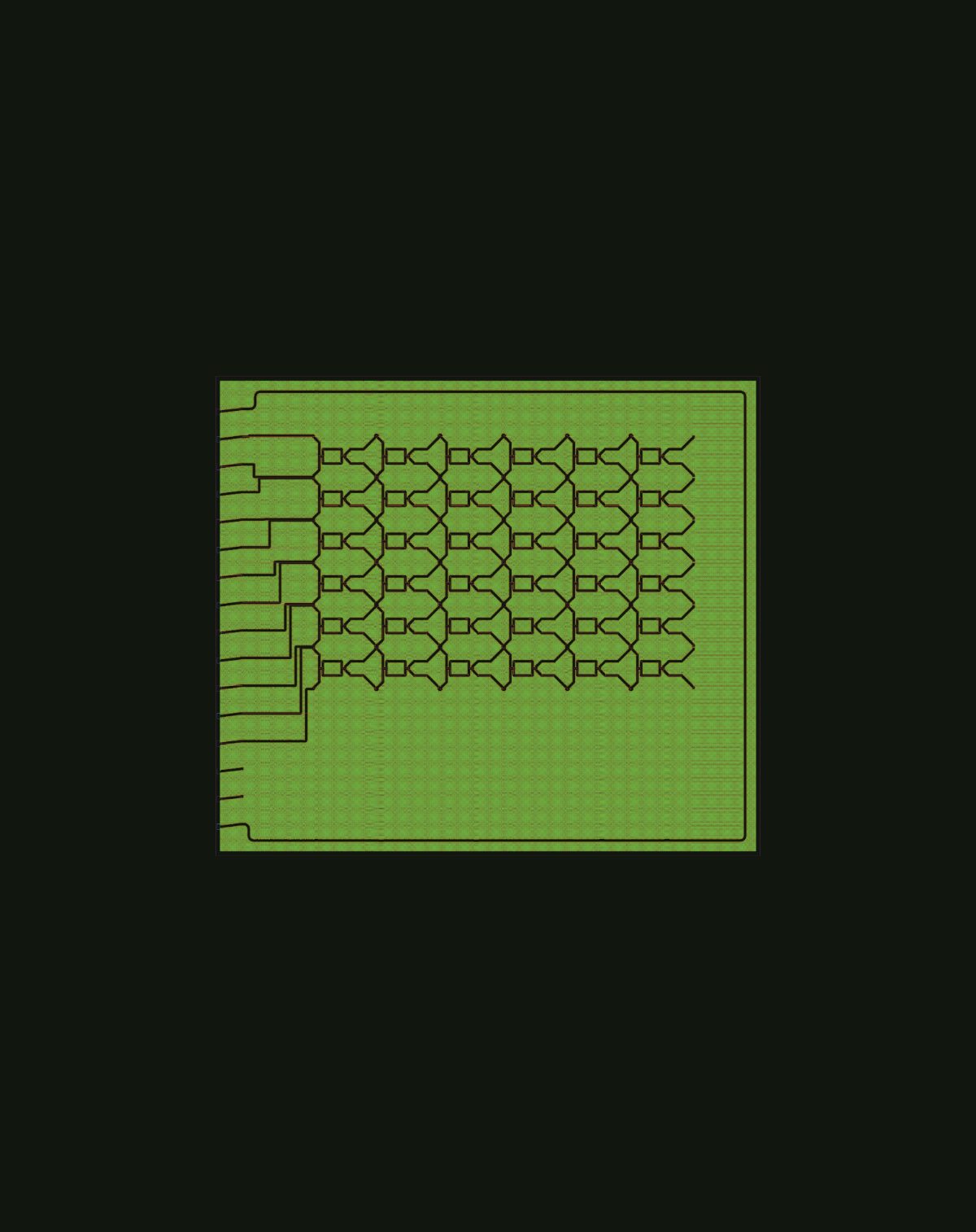
A dense-fill photonic IC with millions of instances. Both layouts load and pan at 60 FPS in a browser tab; these are real screen captures.
Our software, PhotonForge, helps engineers design photonic chips, and we increasingly drive simulations and layouts headlessly. Like much of the field, we use KLayout to inspect those layouts. It has a deep feature set and a strong community behind it.
What has changed is that more of this work now runs without a person at the screen. But seeing a layout stays critical, for humans and for AI agents alike. An agent has to look at what it just built before it decides what to do next, and we have to be able to look with it.
For that reason, our engineering team, with deep expertise in computational geometry, had already built the foundation: the LiveViewer, PhotonForge’s browser-based layout viewer, a modern surface an AI tool can open over a URL and drive. That foundation held comfortably to around half a million shapes.
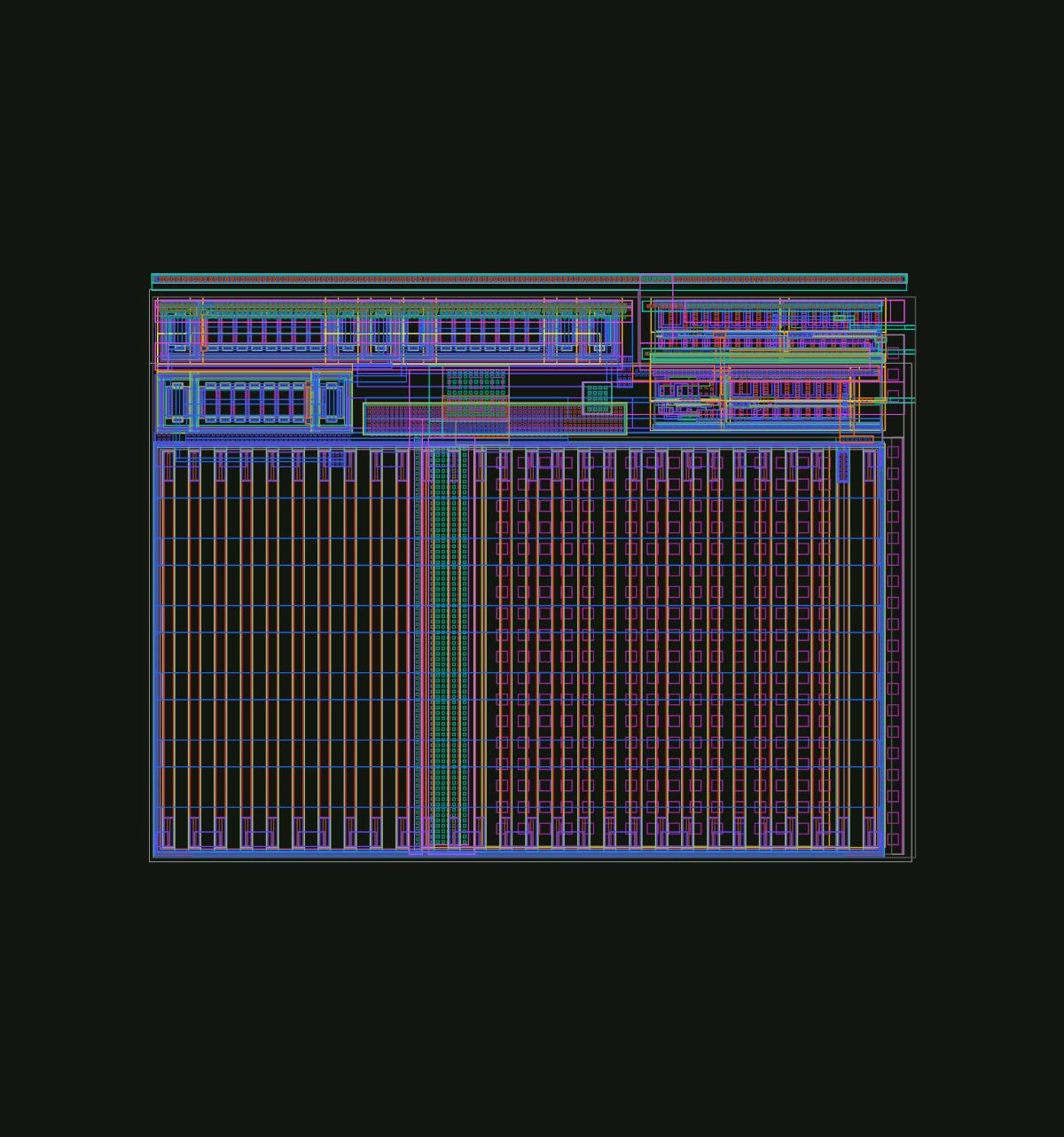
A reference electronic chip, 38 process layers, and a few thousand shapes. Layouts at this scale rendered comfortably on the original browser foundation.
Where it broke
Then we pointed it at the files we actually work with: a photonic test chip with flattened cells and heavy fill, and the Efabless Caravel system-on-chip on SkyWater sky130. We pulled Caravel straight from its public repository so we could open the same GDS in KLayout and in our viewer.
The Caravel die flattens to 38,087,026 shapes, and our dense-fill photonic chips reach several million instances once the fill is in. On files like these, the foundation gave way: the tab froze during load, the renderer ran out of memory and the browser killed the process, and layouts that did load crawled when we panned.
This is not a small-tool problem. At this scale, even a workhorse like KLayout struggles with the same GDS, drawing the Caravel die at roughly one frame per second.
Loop engineering
This is where we took the problem and applied loop engineering. The principle is straightforward: define a clear figure of merit, then let the agent iterate toward it on its own, taking an action, observing the result, verifying that the layout still renders correctly, and adjusting until it meets the goal.
Our figure of merit was two numbers under one constraint: entity count and sustained frame rate, both under a fixed memory ceiling.
That ceiling was not a free parameter. Memory grows with entity count on its own, and the structures that accelerate frame rate usually cost memory and upfront computation of their own. On a consumer laptop with finite memory, the three pull against each other, so the agent had to win all of them at once.
We gave the agent the metrics and the means to read them, since the viewer reports its own entity count, frame rate, and heap, and let it run. It worked the cycle methodically, and every step landed in the log. From the first instrumented baseline to a die panning at 60 FPS, the whole loop ran in under a day.
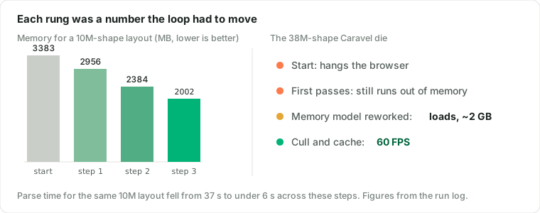
The loop took the 38M-shape die from “hangs the tab” to interactive, one measured step at a time, more than a 70x jump over the half-million baseline.
The result holds at the scale we need to inspect. The full Caravel die now loads in a browser tab and pans at a steady 60 frames per second on a mid-range laptop with no discrete graphics card, both across the whole die and zoomed into a single block. That 60 is the refresh ceiling of the display we tested on rather than a limit of the renderer; the renderer itself measured render rates as high as roughly 120 frames per second, with headroom the display cannot show. On the same machine, KLayout draws the same GDS at about one frame per second.
| Shapes | Pan rate | Renderer headroom | Browser memory |
|---|---|---|---|
| 0.5M → 38M (>70x) | 60 FPS (display-capped) | ~120 FPS | ~2 GB |

Measured live in the browser via the viewer’s own instrumentation. The 60 FPS is the display’s 60 Hz refresh ceiling; the renderer itself measured to roughly 120 FPS.
What an agent does with 38 million shapes

The agent driving test_chip on its own in about ten seconds: open the file, read
the hierarchy, zoom into the MZI array, isolate the waveguide layer, and inspect devices, all
through the same programmatic interface.
An AI agent cannot make sense of 38 million shapes dropped into its context, any more than an engineer can take them in at a glance. It needs the same tools we use to read a layout: pan and zoom to the region that matters, step through the cell hierarchy, toggle layers, and inspect a shape. So we exposed exactly those moves as a small programmatic interface the agent calls directly.
- Pan and zoom. Move the camera and change scale to frame any region, from the whole die to a single device.
setCamera(),fit() - Traverse the hierarchy. Step through the cell tree and choose how many levels to expand, so a million-instance block reads as one cell until the agent wants inside it.
componentTree - Toggle layers. Show or hide any layer to isolate routing, fill, or a single mask.
setLayerVisible() - Select and inspect. Read back the geometry under a point: its layer, size, area, and vertex count.
select(),getState() - Measure. Drop a ruler between two points to check a dimension.
measure()
This is how we build our software, so that humans and agents can drive it the same way. One of the first jobs we gave the agent was visual inspection: open a finished chip and look for the failures a DRC deck does not catch, such as a severed waveguide, a malformed device, or a fill pattern gone wrong. Zoom in, query, judge, move on.
What we learned
Most of the speed came down to culling, deciding what not to draw, and a surprising amount of that turned out to be a visual judgment rather than a numerical one.
You cannot simply drop the small shapes: a chip is mostly small shapes, and culling them makes the layout dissolve into nothing. You have to preserve the aggregate density, the way grains of sand still read as a beach. Other culling is purely about what the eye needs. A marker layer that fills the whole die has to render as an outline when you are zoomed out, or it paints over everything beneath it; that same layer is fine filled in once you are close. We ended up with explicit fill modes, outline, hatch, and solid, because the right answer changes with the view.
Culling only gets you so far, though. Zoom out and the whole die is on screen with nothing left to drop. The usual next move, caching tiles of already-rendered geometry, only pays off while panning: it stutters the moment you reach new territory, and reused tiles scale into visible artifacts as soon as you zoom.
The obvious vector format, SVG, does not really scale either: the vectors are fine, but the renderers fall behind as the entity count climbs. So we wrote our own reactive parsers and renderers, backed by data structures tuned for high-speed drawing, and moved off CPU-heavy spatial indices toward more GPU-friendly algorithms and data structures that bought us both speed and lower memory.
A finished chip is also not a single picture. It is a different rendering at every zoom: a green density field from far out, individual waveguides up close. Both views are correct, only one is exact, and the agent has to know which is which. Making each level of detail honest and legible was as much of the work as raw speed.
Verification mattered as much as the optimization. A figure of merit that rewards only frames per second will converge on a renderer that is fast and draws the wrong chip. The loop produced something we could trust only because every step also confirmed that the geometry still matched, that nothing had been dropped or shifted, before it kept the speed gain. Without that check, it would happily have banked changes that made the viewer faster and the picture wrong.
The bigger takeaway is that loop engineering is a method, not a one-off result. Given a clear figure of merit and an honest way to measure against it, an agent can reach results that are tedious or slow to get by hand, as long as verification stays as rigorous as the optimization. Getting to the solution we have was accelerated by AI, but it still took expert guidance to steer.
We used it to scale a renderer more than 70x, and we expect the same recipe to lift many other parts of how we build our products. We are already excited about the next round of performance work, and there is more to come.
The LiveViewer ships with PhotonForge; to open your own layouts in it, start from the PhotonForge installation guide.
Reference chip: the Efabless Caravel SoC on SkyWater sky130, 277 MB GDS, 38,087,026 flattened shapes, free to clone and open in KLayout or the LiveViewer. Frame-rate, memory, and parse figures were measured in-browser through the viewer’s instrumentation; the KLayout comparison used the same GDS and machine. All screenshots are live captures from the PhotonForge LiveViewer.