On this page The Problem: Bending Light on a Chip
Photonic chips guide light through tiny waveguides etched into silicon, much like electrical wires carry current on a circuit board. These chips are increasingly important for high-speed data links, sensing, and quantum computing. Routing light around corners is surprisingly hard: a smooth 90-degree waveguide bend often needs a radius of several microns to keep loss low, and that takes up valuable chip real estate. What if a computer could design a structure that makes the bend in a fraction of the space?
That’s the idea behind inverse design: instead of designing a device and checking if it works, you specify what you want and let an algorithm figure out the geometry, pixel by pixel, using the same gradient-based methods that train neural networks.
The idea isn’t new. Structural engineers have used topology optimization to design bridges and aircraft parts since the 1980s, and Sigmund’s “99 line topology optimization code” showed the core algorithm fits in a single MATLAB script. This post does the same for photonic inverse design: once the base simulation is given, the core optimization loop fits in ~45 lines of Python.
Let’s build it.
At a glance
Goal
Route 1.0 μm light around a 90-degree bend inside a 3x3 μm design region.
Method
Use Tidy3D’s adjoint gradients to optimize a pixelized material layout with Adam.
Outcome
In ten iterations, the design routes roughly 89% of the power into the desired output mode.
The Problem: Bending Light on a Chip
Light travels through a waveguide, a thin strip of high-refractive-index material (like silicon) surrounded by a lower-index material (like air). The light is confined to the strip by total internal reflection, similar to how fiber optics work.
We want to route light at wavelength 1.0 μm around a 90-degree corner. It enters horizontally from the left and must exit vertically downward. Between input and output sits a design region, a 3x3 μm square where the optimizer can freely place or remove material. The question is: what pattern maximally routes the light from input to output?
To simulate how light propagates through a given geometry, we use Tidy3D, a cloud-based electromagnetic solver. Given a device geometry and material properties, Tidy3D solves Maxwell’s equations and tells us where the light goes. Crucially, Tidy3D exposes an autograd-based inverse-design workflow, which lets us compute gradients through the simulation (more on this in Step 3).
The base simulation (waveguides, light source, output monitor, and absorbing boundary conditions) is pre-built and stored in sim_base.yaml. We load it and focus entirely on the optimization algorithm.
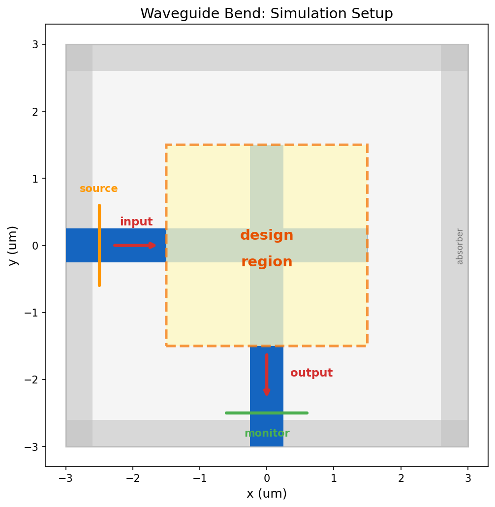
Simulation setup. Light enters from the left through a horizontal waveguide and should exit downward through a vertical waveguide. The dashed box is the design region where we will optimize the material layout.
import autograd
import autograd.numpy as np
import tidy3d as td
import tidy3d.web as web
from tidy3d.plugins.autograd import make_filter_and_project

sim_base = td.Simulation.from_file("sim_base.yaml")
Step 1: From Design Variables to Simulation
We need a function that maps a set of design variables to a complete electromagnetic simulation. Each pixel in the design region gets a variable , a number between 0 and 1. We then convert to a permittivity value. Permittivity is the square of the refractive index and controls how light interacts with the material. Our material has refractive index , so its permittivity is . Air has permittivity 1.
But we don’t map to permittivity directly. Two transformations happen first:
Density filter
A convolutional filter with radius blurs each pixel’s value with its neighbors. This is important because these devices will eventually be fabricated, and real manufacturing processes have a minimum feature size they can reliably produce. The filter ensures no feature in our design is smaller than , acting as a simple proxy for more sophisticated fabrication-aware design checks. We use .
Tanh projection
After filtering, a tanh function pushes the smoothed values toward 0 or 1, controlled by a sharpness parameter . At low , the mapping is nearly linear, so the optimizer can explore intermediate values freely. At high , it becomes a hard threshold that forces every pixel to be pure material or pure air.
The figure below shows the effect of these two transformations applied to random noise. Filtering smooths out fine features; projection pushes values toward binary. When applied during optimization, they guide the optimizer toward clean, fabricable geometries.
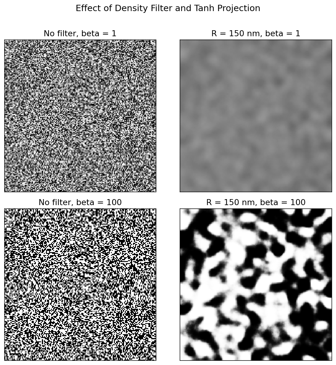
Filtering and projection. Filtering suppresses arbitrarily small features, while increasing beta pushes the design toward a binary material-air pattern. We use both together during optimization.
n_mat = 2.0                    # material refractive index
eps_mat = n_mat ** 2           # permittivity = n^2 = 4.0
design_size = 3.0              # design region side length (um)
pixel_size = 1.0 / 50          # pixel resolution (um)
radius = 0.150                 # filter radius R (um), sets minimum feature size
nx = ny = int(design_size / pixel_size)

design_region_geo = td.Box(center=(0, 0, 0), size=(design_size, design_size, td.inf))

filter_project = make_filter_and_project(radius=radius, dl=pixel_size)
Now we construct the function that takes our design parameters , applies the filter and projection to get a permittivity map, builds a structure from it, and adds it to the base simulation we loaded from file.
def make_sim(params, beta):
    """Map design variables through filter, projection, and into a simulation."""
    density = filter_project(params, beta=beta)
    eps_data = 1.0 + (eps_mat - 1.0) * density
    structure = td.Structure.from_permittivity_array(
        eps_data=eps_data, geometry=design_region_geo,
    )
    return sim_base.updated_copy(
        structures=list(sim_base.structures) + [structure],
    )
Step 2: Objective Function
We need a single number that tells us how well the device works. At the output waveguide, Tidy3D measures the mode amplitude , a complex number describing how much light couples into the waveguide’s guided mode. The power carried by that mode is , so our figure of merit is simply the output mode power:
A perfect device would have (all input power reaching the output). In code: we build a simulation from our design variables, run it on the cloud, extract the mode amplitude, and return the power.
def objective(params, beta):
    """Run electromagnetic simulation and return output mode power."""
    sim = make_sim(params, beta)
    data = web.run(sim, task_name="invdes", verbose=False)
    amps = data["mode"].amps.sel(direction="-", mode_index=0).values
    return np.sum(np.abs(amps) ** 2)
Step 3: Gradients via the Adjoint Method
To optimize, we need the gradient for every pixel: how does tweaking the value of each pixel affect the output power? The brute-force approach would perturb each pixel one at a time and re-simulate. For our 150x150 grid, that’s 22,500 simulations per optimization step. Completely impractical.
The adjoint method computes the exact same gradient using just two simulations, regardless of how many pixels there are:
- Forward simulation: run the device normally, injecting light at the input and recording the electric field everywhere. This is the simulation we’d run anyway to evaluate the design.
- Adjoint simulation: inject a special source at the output monitor that encodes the derivative of our objective function. This tells the simulation “how much does the objective change if the field here changes?” The resulting adjoint fields propagate backward through the device.
After both simulations, the gradient at each pixel is simply the overlap of the forward and adjoint electric fields:
Two simulations instead of 22,500. Intuitively, the forward field tells you “how strongly does this pixel interact with the input light?” and the adjoint field tells you “how strongly does this pixel influence the output?” Their product gives the sensitivity of the objective to each pixel.
This is the same principle behind backpropagation in neural networks. The adjoint simulation is the vector-Jacobian product (VJP) of the forward electromagnetic solve, and both exploit the chain rule to avoid redundant computation (see Minkov et al., 2020 for a detailed treatment connecting adjoint methods and automatic differentiation in photonics).
Tidy3D implements the adjoint math as the VJP of its electromagnetic solver, so this second simulation happens automatically behind the scenes. When we wrap our objective in autograd.value_and_grad, Tidy3D runs both the forward and adjoint simulations and backpropagates the gradient through the entire computational pipeline (simulation, mode decomposition, filter, projection, and all).
val_and_grad = autograd.value_and_grad(objective)
# val_and_grad is a function: given (params, beta), it returns (fom, gradient)
# e.g. fom, grad = val_and_grad(params, beta=10)
Step 4: Optimize
With cheap gradients in hand, we can use any gradient-based optimizer. The autograd library provides Adam out of the box. Adam is the same optimizer that trains most neural networks: it maintains running averages of the gradient (momentum) and its square (adaptive learning rate), giving more stable convergence than plain gradient ascent.
Adam’s grad function takes (params, iteration). We use the iteration number to gradually increase : early on, a low keeps the design continuous, giving the optimizer freedom to explore many possible solutions; as the design matures, we ramp up to push toward a binary (material or air) structure that can actually be fabricated. We also negate the gradient so that Adam maximizes our objective instead of minimizing.
from autograd.misc.optimizers import adam

n_steps = 10
params0 = 0.5 * np.ones((nx, ny, 1))
history, param_history = [], [np.array(params0)]

def neg_grad(params, i):
    """Negative gradient with projection schedule (Adam minimizes, we negate to maximize)."""
    params = np.clip(params, 0, 1)
    beta = 5 + 45 * i / max(n_steps - 1, 1)
    fom, g = val_and_grad(params, beta)
    history.append(float(fom))
    param_history.append(np.array(params))
    print(f"  step {i:2d} | FOM = {fom:.4f} | beta = {beta:.1f}")
    return -g
Run It
Starting from a uniform design ( everywhere, halfway between air and material), the optimizer discovers the structure from scratch. Each step runs two simulations on the cloud (forward + adjoint), computes the gradient across all 22,500 pixels, and updates the design.
params_opt = np.clip(adam(neg_grad, params0, num_iters=n_steps, step_size=0.3), 0, 1) step 0 | FOM = 0.0022 | beta = 5.0
step 1 | FOM = 0.0531 | beta = 10.0
step 2 | FOM = 0.3975 | beta = 15.0
step 3 | FOM = 0.3932 | beta = 20.0
step 4 | FOM = 0.6367 | beta = 25.0
step 5 | FOM = 0.7139 | beta = 30.0
step 6 | FOM = 0.7795 | beta = 35.0
step 7 | FOM = 0.8487 | beta = 40.0
step 8 | FOM = 0.8861 | beta = 45.0
step 9 | FOM = 0.8856 | beta = 50.0Results
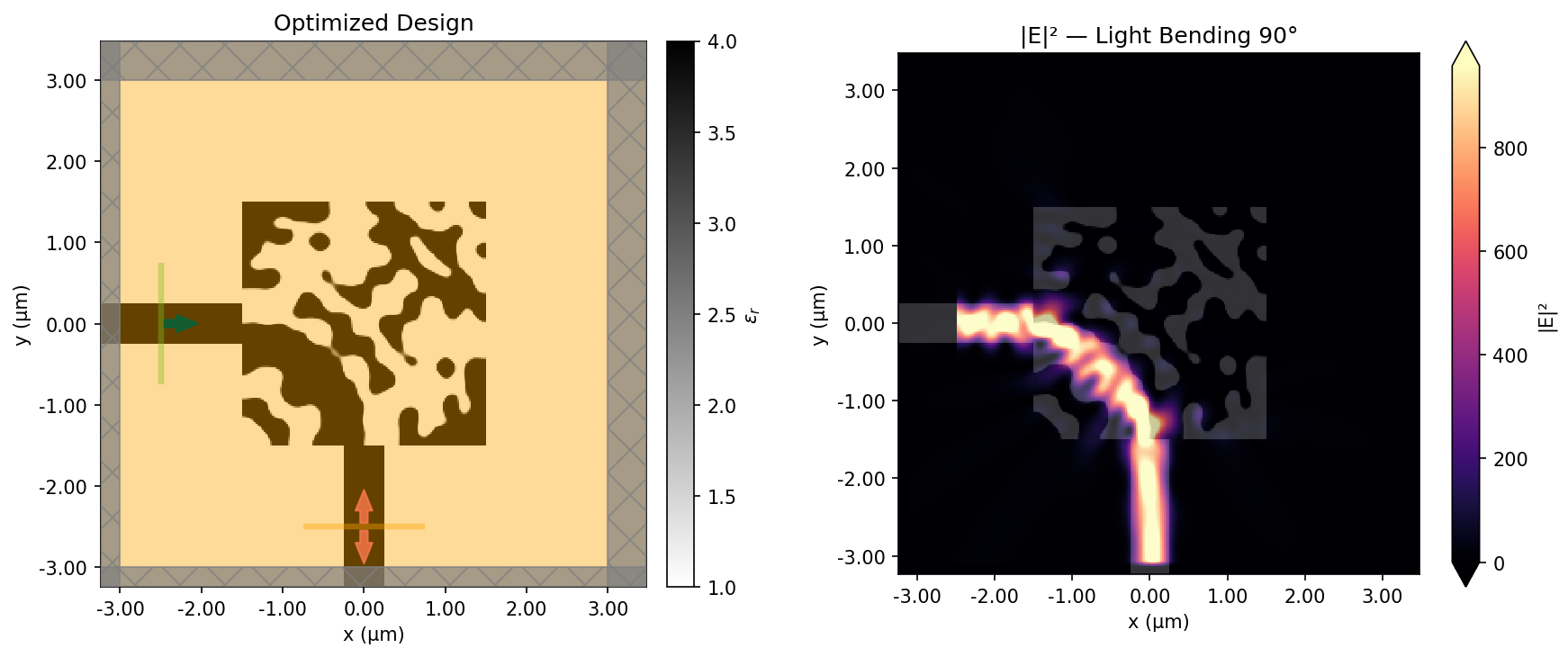
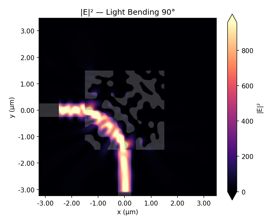
Final device and field response. The optimized permittivity pattern comes first, with dark regions showing the high-index material and the light background showing air. The corresponding field intensity, |E|^2, shows light entering from the left and bending downward into the output waveguide.
The final design looks nothing like what a human engineer would draw. There’s no smooth curve, no gradual taper. Instead, the optimizer found a pattern of material and air that manipulates the electromagnetic field through interference to route the light around the corner.
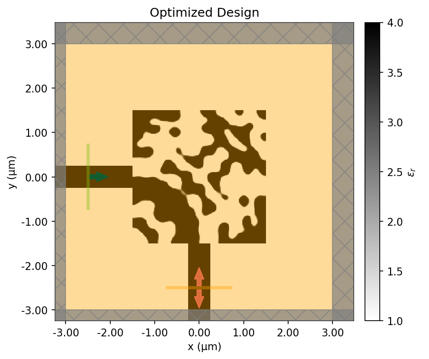
Design evolution
Watch the design emerge from a uniform gray starting point. Early steps explore broadly (low , soft features); later steps sharpen into a clean binary design (high ).
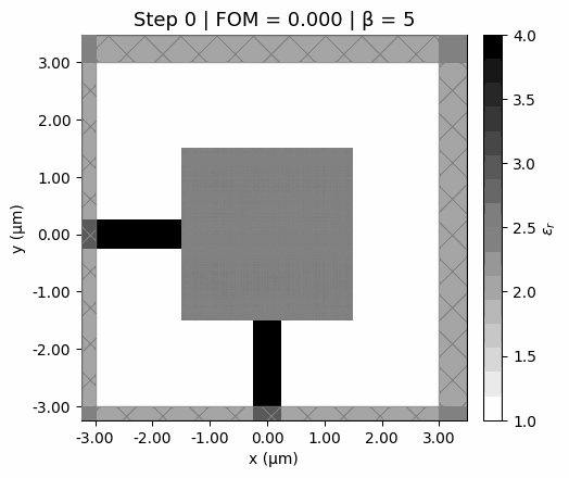
Optimization trajectory. The design starts from a uniform gray initialization, develops structure quickly in the early low-beta steps, and then sharpens into a binary pattern as the projection becomes steeper.
Convergence
The animation shows how the geometry sharpens visually. The convergence trace shows the same story numerically: rapid early gains, then diminishing returns as the design binarizes.
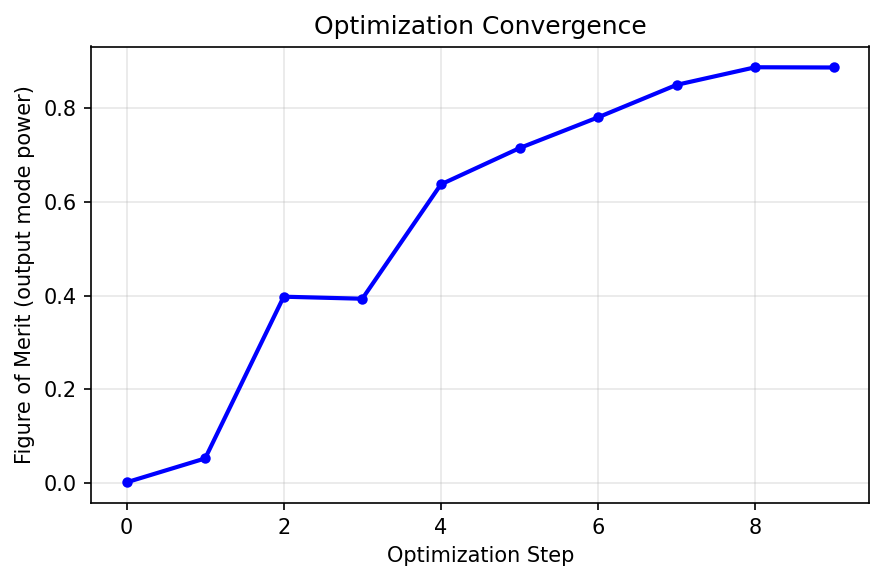
Convergence. The output-mode power rises quickly once the optimizer finds the basic routing pattern, then levels off as the design binarizes.
The Complete Pipeline
Zooming out, each optimization step does the same five things in order:
01
Filter and project
Map the raw design variables into a smooth, increasingly binary material distribution.
02
Build the simulation
Insert that material layout into the pre-built Tidy3D model of the waveguide bend.
03
Run the forward solve
Compute the output-mode power, which becomes the figure of merit.
04
Run the adjoint solve
Backpropagate sensitivity information through the electromagnetic simulation.
05
Update the design
Use Adam to take a gradient step, then repeat with a slightly sharper projection.
Each iteration costs two electromagnetic simulations. The adjoint method makes this feasible. Without it, we’d need 22,500 simulations per step instead of 2.
Going Further
This post is a basic introduction to the technique, but a functional one. There are many more advanced variations for real problems in photonic device design. Production systems add:
- 3D simulations: real devices have finite thickness and vertical confinement
- Broadband optimization: performance across a range of wavelengths, not just one
- Fabrication constraints: minimum feature sizes, curvature limits, etch profiles
- Multi-objective: multiple output ports, polarizations, robustness to manufacturing variation
If you’re interested in going deeper, check out these resources:
- Inverse design examples (wavelength demultiplexers, metalenses, mode converters, and more)
- Inverse design quickstart notebook (a more complete worked example using the same autograd workflow)
- Inverse design learning center (course-style introduction to adjoint optimization in Tidy3D)
Want the exact working files for this post? Download the companion bundle. It includes the notebook, the Jupytext script export, sim_base.yaml, and the helper script that rebuilds the base simulation. Re-running the optimization requires a Tidy3D account.