On this page Background
Inspired by the recent hype around autoresearch loops with AI agents, I decided to explore a simple question:
If you give agents access to a well-defined photonic component design problem, a local electromagnetic simulator, and a fabrication constraint checker, could they reliably design photonic devices on their own, just by iterating on geometries?
To my surprise, the answer was a resounding yes! The agents were able to create a handful of common photonic components, with designs that met our performance criteria and were simple and intuitive. There were some caveats and surprising results though, which we’ll get into later. For now, let’s dive into the problem setup and show what the agents came up with.
Background
Photonic integrated circuits route light through structures etched on a silicon chip, much like electronic circuits route current through wires. Light can carry far more information than electronic signals and with very low power loss. As a result, photonic technologies are playing an increasingly important role in improving performance of computing platforms for AI and other applications. These photonic devices are composed of many components, such as waveguides, splitters, filters, etc., which help guide the light around the chip. Engineering these components is hard because, unlike with electrons, the wave nature of light needs to be accounted for in the design. Even small geometry changes can scatter light, create unwanted reflections, or couple power into the wrong mode.
A standard approach is to use a simulator for Maxwell’s equations to model and optimize the device. One such algorithm is FDFD (finite-difference frequency-domain), which discretizes Maxwell’s equations on a grid and solves for the steady-state field pattern at a given frequency. You define the geometry and materials, pick a wavelength, launch light into the simulation, and measure what comes out the other end. The figure of merit (FoM) is typically a mode overlap, which measures how much of the output light matches the desired profile on the other side of the device.
One can use simulation combined with optimization techniques like gradient descent or parameter sweeps to come up with a candidate device. But a device that looks great in simulation may be impossible to fabricate since these structures are so small (typically features are measured on the tens of nanometers scale). Foundries impose design rule checks (DRC): minimum feature width, minimum gap between features, minimum area, no tiny holes. A design that scores well in simulation but violates DRC is useless. In our case, we chose a minimum feature size of 300 nm — more relaxed than typical foundry PDKs, which often enforce 150–200 nm, but strict enough to impose meaningful constraints.
Therefore, the real problem for any photonic device designer is: find a geometry that maximizes the photonic objective while passing foundry design rule checks!
Problem Statement
We wanted to explore whether we could automate this design process, with a simulator, a DRC engine, and a few well-defined design problems.
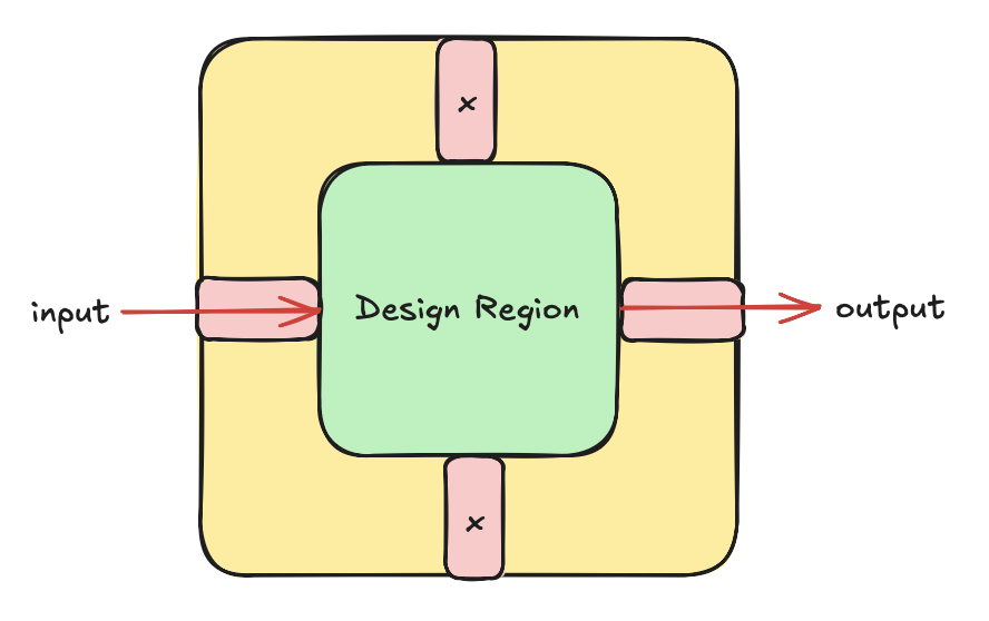
For a given design problem, each agent got the same interface:
- They can submit designs as a list of geometric objects. These can be anything (polygons, pixelated grids, etc.).
- We compute the scalar figure of merit for this submission using a fast, local electromagnetic solver.
- We check whether this geometry passes a basic design rule check (DRC).
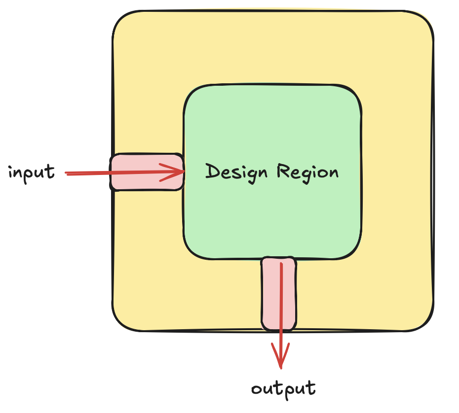
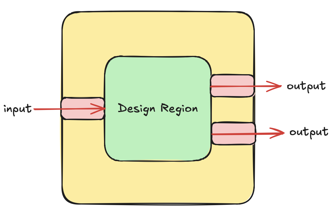
- We make sure all geometries provided are within a “design region”.
Given the figure of merit and acceptance criteria, we evaluate the submission and instruct the agent to continue iterating until a suitable design is found. The challenge is defined in a repository that makes it reusable: a challenge wrapper, evaluator, autoresearch harness, and leaderboard. The whole setup was designed so that any agent can enter this directory, read the prompt, and begin submitting solutions. As the agents work, they create visual artifacts: geometry visualizations, electromagnetic field profiles. The agents can see each other’s previous submissions, in fact they often used them!
Let’s walk through what happened. We ran two agents, Claude Opus 4.6 and OpenAI GPT 5.4, on four challenges of increasing difficulty — from a simple waveguide bend up to a three-channel wavelength demultiplexer. Both agents could see each other’s submissions.
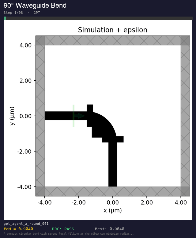
Experiment 1: 90-Degree Bend
We often need to steer light around on photonic circuits, so having the ability to bend light on chip is a critical functionality. However, if you make such a bend too sharp, the light will tend to leak out.
Problem: Route light from a horizontal waveguide to a vertical waveguide through a 90-degree turn in a design region.
FoM: What fraction of light makes it to the vertical output waveguide? Perfect score = 1.0.
Starting point: A naive, circular arc bend with matching sections and a corner pad, FoM = 0.904.
Design Process
The agents first performed a general test of several different candidate geometries. Claude tested 14 diverse geometries (Euler bends, corner mirrors, MMI regions (“multi-mode interference” regions), chamfered L-bends) and noticed that simply widening the arc from 0.50 to 0.70 μm beat everything else. GPT arrived at the same conclusion through a more incremental path, starting by tuning the size of rectangular pads at the bend junctions and progressively stripping away decorative geometry until we were left with a simple bend again with a variable width.
Bend design progression. Both agents converge from diverse initial geometries toward a simple variable-width arc.
With the basic strategy in place, both agents naturally progressed to a second stage: fine tuning the geometry through parameter sweep. Both agents independently swept the width of the bend and found that 0.75–0.80 μm was the sweet spot for a uniform-width arc with a corner pad. But things got interesting as they tried pushing further and ran into constraints.
DRC Violation: Wider arcs without the pad gave raw FoM up to 0.977, but failed DRC because the gap between the wider arc and the 0.50 μm arm waveguides at the junction dropped below 300 nm. Both agents hit this wall and both found the same way around it.
Solution - Variable-width arcs: Instead of a uniform-width arc, the agents decided to use one that starts at the arm width (0.50 μm) at the ports and smoothly widens at the bend apex. This solves two problems simultaneously: no DRC gap at the ports (width matches the arms exactly) and reduced radiation at the apex (wider waveguide confines the mode better).
Claude used a sinusoidal width profile and found the optimal apex width at 0.65 μm. GPT used a power-law profile with a tunable exponent and found a similar optimum at 0.648 μm with exponent 0.79. Both reached FoM ≈ 1.0 — effectively perfect transmission in the 2D single-wavelength simulation.
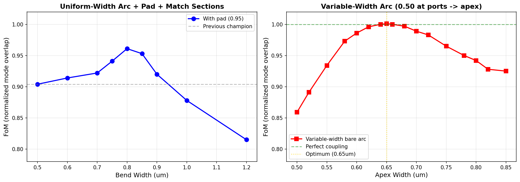
Width sweep results. Both agents independently find that a variable-width arc near 0.65 μm apex width maximizes transmission.
Winning bend. Claude’s variable-width arc achieves FoM ≈ 1.0 with a single polygon.
Result
Both agents achieved FoM ≈ 1.0 with a single bare polygon. The winning design family is a variable-width quarter-circle arc: where peaks at the 45-degree apex and returns to zero at the ports.
And just to reiterate: this was all done 100% autonomously! The agents came up with the candidate geometries, swept parameters, and corrected the DRC violations all without intervention.
This was about as simple as it gets for a design problem, so the result is interesting but not groundbreaking: the agents found a good parameterization through experimentation and then swept parameters to optimize. Next we tried some harder problems.
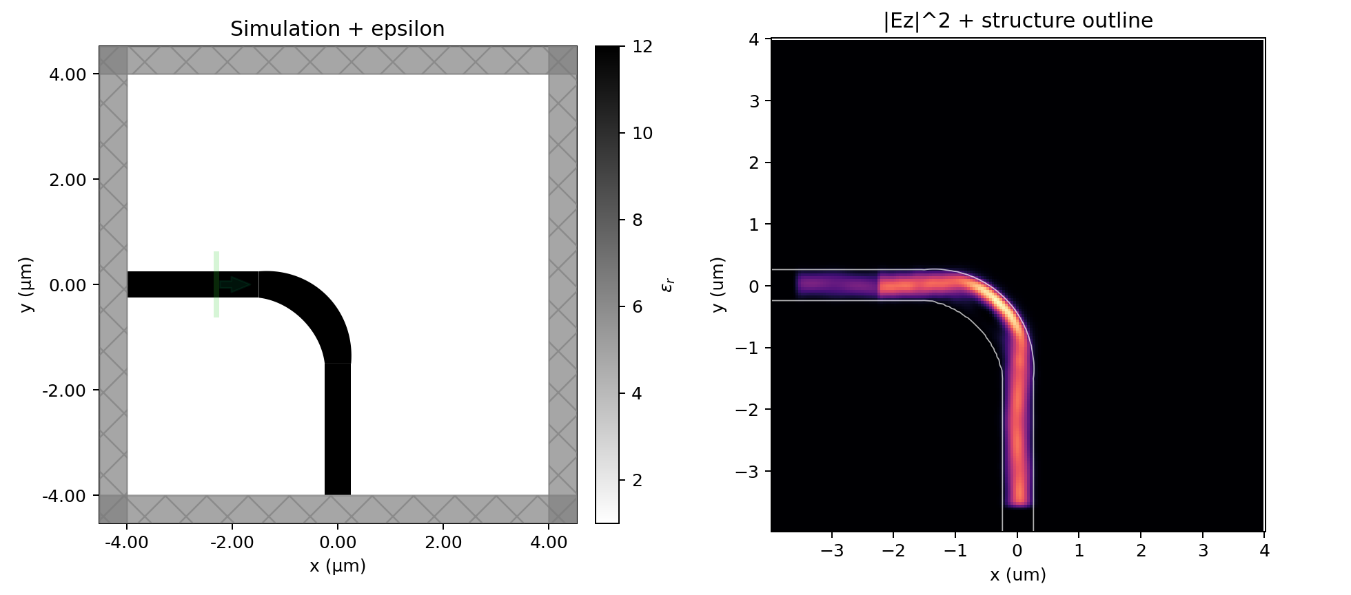
Experiment 2: Waveguide Crossing
Often when designing complex circuits, we need waveguides to cross so we can connect components together. Since this is all happening on a single plane, we need crossing components that allow the light to pass through without any power leaking into the perpendicular section.
Problem: Pass light straight through a intersection where two orthogonal waveguides cross, minimizing crosstalk into the perpendicular waveguide. The design should have 90-degree rotational symmetry.
FoM: . Basically balancing through transmission and adding an explicit extra penalty for crosstalk. Perfect score = 1.0.
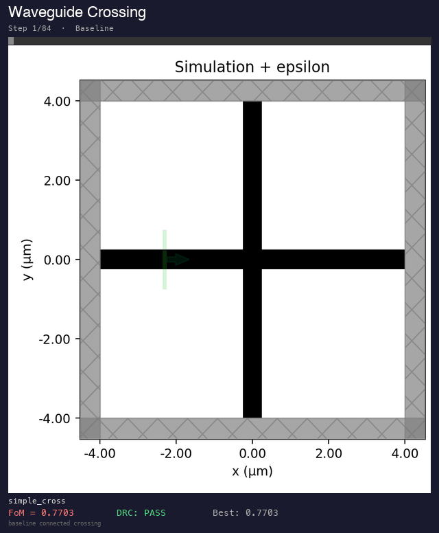
Starting point: A simple plus-shaped cross (two perpendicular waveguides), FoM = 0.770.
Design Process
Claude tested circles, diamonds, ellipses, MMI regions, tapered transitions, and variable-width crosses. Every expansion at the intersection made things worse: circle (0.375), diamond (0.553), ellipse (0.517), square MMI (0.623).
Crossing design progression. The agents explore a wide range of intersection geometries before converging on a widened cross.
GPT started by adding a wider central cross and found that this solution worked well off the bat. After it tuned parameters, the optimal uniform width was found to be right around 0.75 μm (FoM = 0.962).
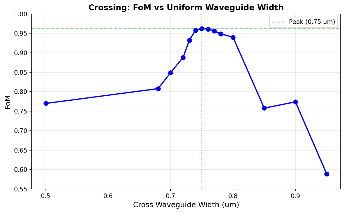
Crossing width sweep. The sharp peak at 0.75 μm reveals a self-imaging condition — small geometry changes degrade performance quickly.
The sweep curve shows that the device is quite sensitive: 0.74 or 0.76 drops the FoM by 0.003. From looking at the field plots, we can see that this is because of a self-imaging condition in the center intersection region: the width is chosen so that the light in the junction interferes constructively at the output after crossing the perpendicular waveguide. This interference is inherently sensitive to any changes in the geometry, so it’s not a great design.
After some more prodding, GPT then found an improvement: adding another ~0.95 μm square dielectric pad at the center of a 0.74 μm cross (FoM = 0.968). Claude independently converged to the same design family, achieving 0.968 with a Gaussian-flared cross and a 0.96 μm pad. The two agents tied within solver noise.
Result
FoM = 0.968 (both agents). The optimal crossing is a 0.74 μm wide cross with a square center pad. Unlike the bend, variable-width (polygon) approaches didn’t help — the crossing relies on a self-imaging condition that requires a well-defined multimode section. The center pad is the only refinement that provides a measurable improvement.
The takeaway from this: the crossing problem is almost entirely solved by only three parameters: the sizes of the rectangles in the design region. This shows that devices can work well with just a small number of good knobs and disciplined iteration — and the agents figured that out on their own.
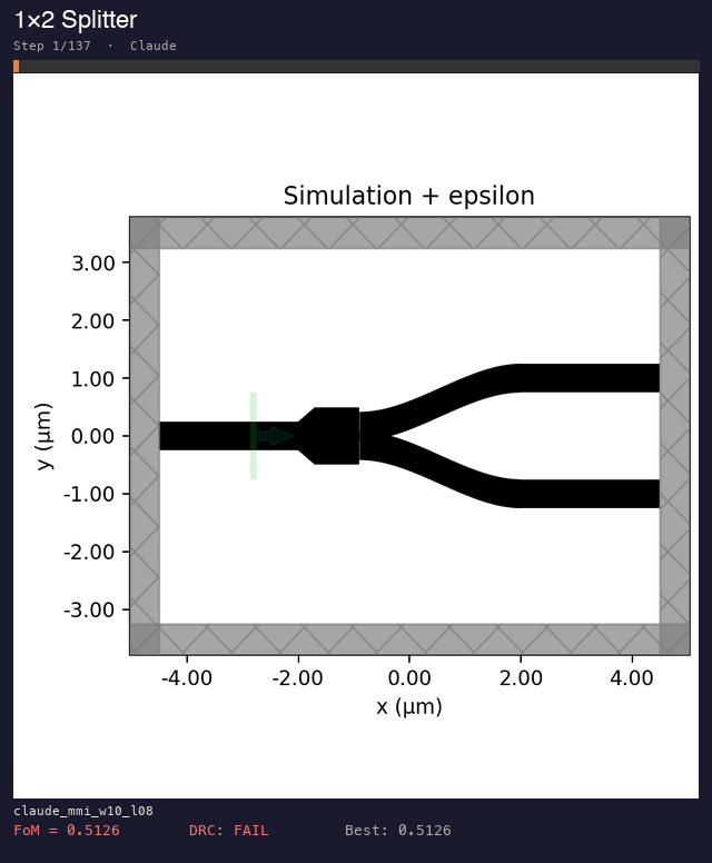
Experiment 3: 1×2 Splitter
It is important to be able to split the power in a waveguide into two or more arms so we can do routing or interfere the light with itself later on. A 1×2 splitter is a very common photonic component that seeks to do a 50-50 split with very low loss.
Problem: Split light from one input waveguide equally into two output waveguides separated by 2.0 μm, in a design region.
FoM: , rewarding balanced 50/50 splitting via the geometric mean. Perfect score = 1.0.
Starting point: A big rectangle filling the design region, FoM = 0.507.
Design Process
This was the hardest challenge of the three (so far):
Splitter design progression. The agents iterate through Y-branches, separated arms, and tapered designs.
Both agents immediately tried Y-branches: simply taper the input section into two curved output arms. Claude’s smooth Y-branch with cubic Hermite S-curves got FoM = 0.966, nearly perfect. GPT’s initial Y-branches were similarly strong. But they all failed DRC. The two arms at the split point have zero gap, violating the 300 nm minimum.
The agents then struggled to fix the DRC violations; they both pre-separated the arms by 300+ nm at the split point and added tapers to feed both arms. The forced gap scattered light because the single-lobed taper mode didn’t match the two-lobed arm mode. Claude’s best separated Y reached FoM = 0.812 after sweeping the split point position.
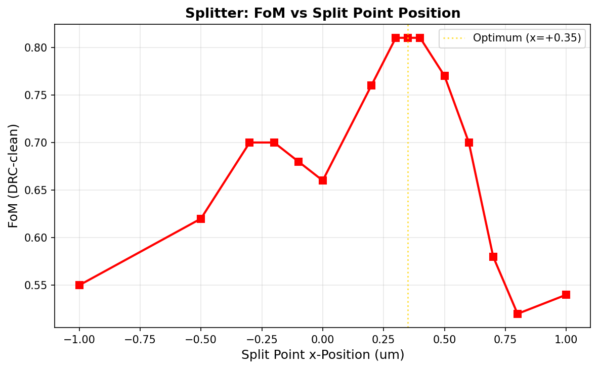
Split-point sweep. Claude’s best DRC-clean separated Y reaches FoM = 0.812 at the optimal split position.
GPT continued iterating on the separated Y family and discovered a parameterization that Claude missed. After the split, it kept the arms wide for a short section before tapering them back to the output width. This let the wider arms better capture the splitting mode before narrowing down. GPT also tuned the arm width independently (0.57 μm instead of 0.50), brought the gap size down to the minimum of 300 nm, and added a width-exponent parameter controlling how aggressively the arms taper.
The result was FoM = 0.906, which was a significant jump past Claude’s 0.812 and into territory that Claude couldn’t reach with the simpler parameterization.
Claude also tried:
- MMI splitters: a 2D sweep of 42 width/length combinations found FoM = 0.963 but failed DRC
- Directional couplers (0.221)
- Pixelated shapes (0.676) using adjoint optimization — though this likely reflects a limited optimization setup rather than a fundamental limitation of adjoint methods.
But none of these matched GPT’s result.
Result
FoM = 0.906 (GPT’s hold-and-taper Y-branch) was the best DRC-clean result. Claude’s best was 0.812 with a simpler parameterization. The raw (DRC-violating) Y-branch reached 0.966 for both agents. The 300 nm DRC gap constraint at the split junction was a major challenge.
Lessons
The splitter was fundamentally different from the bend and crossing. Both the bend and crossing were single-input single-output problems where light stays in one continuous structure. The splitter requires light to transition from one waveguide to two separate waveguides, and DRC forces a minimum gap at that transition.
The gap between DRC-clean and DRC-free performance (0.906 vs. 0.966) was where the real engineering challenge lives. GPT’s hold-and-taper design showed that there’s still room for better parameterizations: the splitter rewarded more knobs than the bend or crossing did. This is the device where the agents’ search strategies diverged the most, and where GPT’s more incremental, parameter-by-parameter approach paid off.
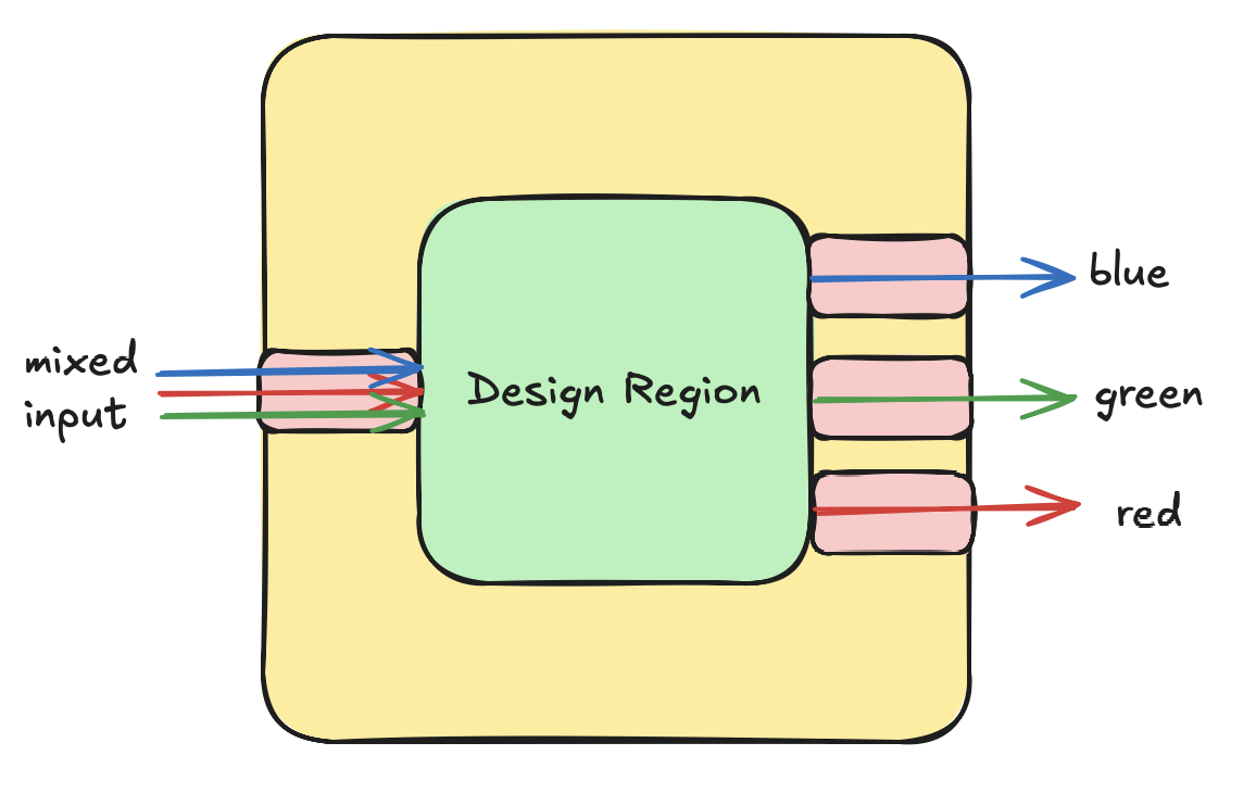
Experiment 4: 3-Channel Wavelength-Division Demultiplexer
The bend, crossing, and splitter were all single-wavelength, single-mode problems where the agent proposes a shape, gets a score, and iterates. They could be solved by parametric sweeps in low-dimensional design spaces where one or two dominant parameters (bend width, crossing width, split position) determine most of the performance.
Next, we tried a more challenging problem involving wavelength selectivity, where the conventional geometric approaches failed miserably.
Many photonic devices end up splitting information into different wavelength channels (wavelength division multiplexing), which allows them to process more information in parallel. Being able to split and recombine these wavelengths is a major challenge. In this design challenge, we had a single input containing light with a mix of three different wavelengths (1.45, 1.55, 1.65 μm) and tried to design a single device to direct each of these wavelengths to one of three separate output ports (top, center, bottom) through a design region.
FoM: Average normalized transmission into the correct output port across all three channels. Perfect score = 1.0 (each wavelength fully routed to its target).
Design Process
Every parametric approach, whether proposed by the agents or designed by hand, scored below 0.5:
- Simple MMI box: 0.016 (splits power but doesn’t route by wavelength)
- 3-way Y-branch: 0.24 (splits equally, no selectivity)
- Direct connect (straight + S-bends): 0.315 (good through, poor drops)
- Offset MMI, asymmetric tapers, random structures: all below 0.45
The approach that (somewhat) worked was to break the design region into a grid of pixels, each with a material density between 0 and 1. Think of this as similar to a “material density” image. Starting from uniform grey (0.5), gradient-based optimization iterated on the pixels for 60 steps of Adam optimization and reached FoM = 0.935, an approach similar to training ML models. The optimizer found a complex density pattern that creates different interference pathways for each wavelength, routing each to its correct output port.
But this design did not pass DRC. The pixel-based structure contains sub-wavelength features, tiny gaps, and isolated islands that no foundry would accept. And it was not binarized properly.
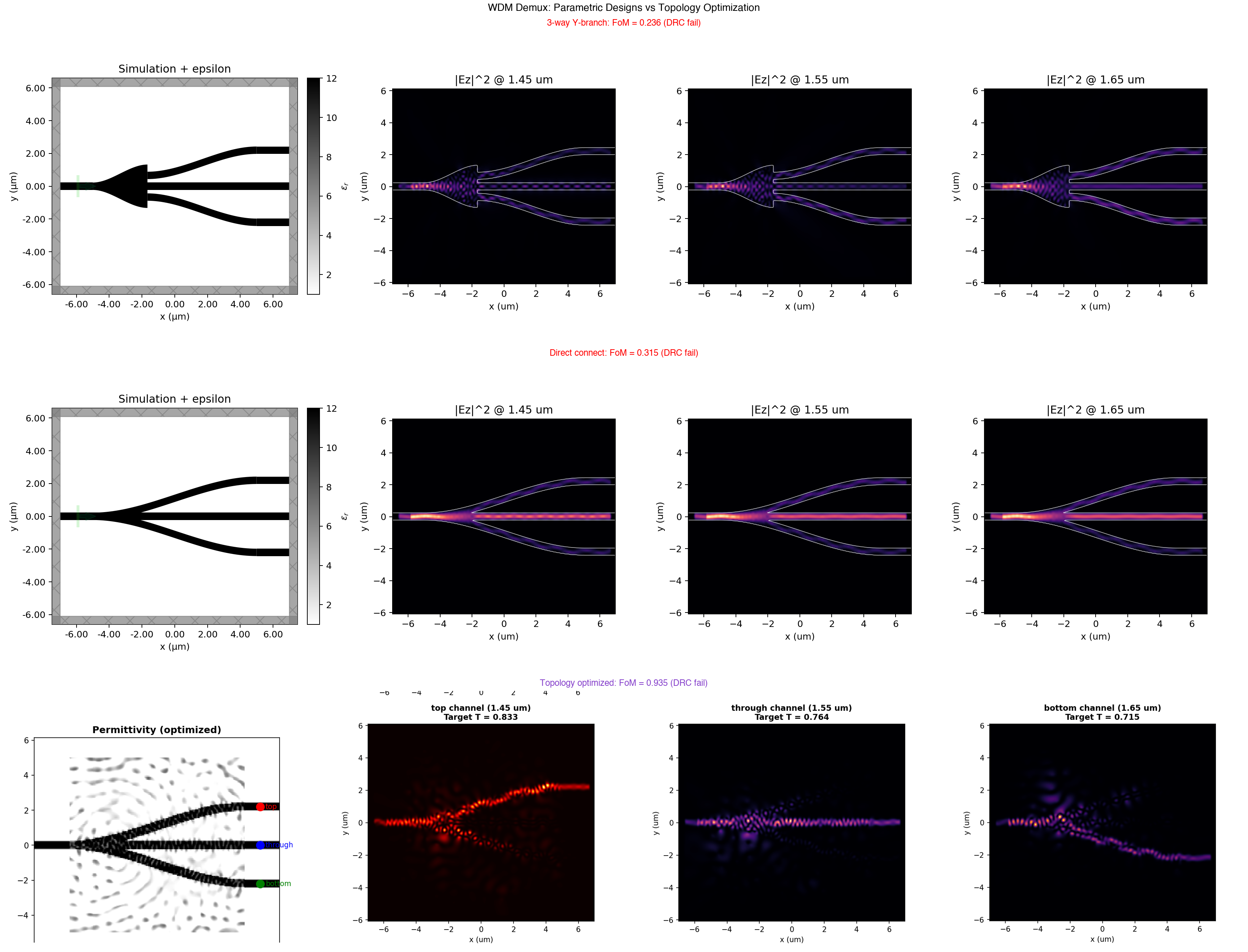
Demux simulation reports. The pixel-based density optimization routes each wavelength to its target port, but the resulting structure violates DRC.
We’ll explore this approach in a follow-up blog. But the takeaway was that the demultiplexer seemed to be a problem too challenging for the agents to tackle while passing DRC at this stage.
Summary
| Challenge | Baseline | Geometric Parameters | Pixel-Based Density | DRC |
|---|---|---|---|---|
| Bend | 0.904 | ≈1.0 | N/A | PASS |
| Crossing | 0.770 | 0.968 | N/A | PASS |
| Splitter | 0.507 | 0.906 | N/A | PASS |
| 3-ch WDM demux | 0.016 | 0.315 | 0.935 | FAIL |
Takeaways
Both agents converge on the same physics (with a caveat)
For the bend and crossing, Claude and GPT arrived at the same optimal design families. The variable-width arc for the bend and the widened cross for the crossing exploit properties of the physics that a photonic designer could understand.
However, an important caveat: the agents could see each other’s previous submissions throughout the challenge, and they used this. I found Claude regularly taking inspiration from GPT’s designs and proposing variations on them. So the convergence is not purely independent. The shared leaderboard acted as a forum for them to communicate. The fact that both agents ended up at the same designs is encouraging, but it’s weaker evidence than if they had converged in complete isolation. A cleaner experiment would run each agent in a separate sandbox with no visibility into the other’s submissions.
Parameterization matters far more than search strategy
The splitter was the exception. GPT’s hold-and-taper parameterization (six tunable parameters: split position, gap, arm width, center exponent, hold fraction, width exponent) explored a richer design space than Claude’s three-parameter separated Y. The extra degrees of freedom turned out to matter: they let the optimizer find designs that better balance the physics of mode splitting against the DRC gap constraint.
DRC is the binding constraint
In all three challenges, the best raw designs (ignoring DRC) significantly outperformed the best DRC-clean designs. The fabrication constraint is what limits performance. Both agents spent more iterations working around DRC failures than optimizing the actual photonics. A lot of the failed designs were not bad ideas, they were ideas that did not survive the interaction between wave physics and fabrication constraints. It is important therefore to consider a systematic way to incorporate DRC validity into the geometry generation process.
Simple designs win (for easy problems)
The bend champion is only one polygon. The crossing champion is two rectangles. The splitter champion is three polygons. Every attempt at complex multi-structure designs (corner mirrors, MMI regions, directional couplers, resonant cavities) performed worse than simple, well-tuned geometries. For simple problems, the best solutions were not inventive shapes but rather simple parameterizations.
Simple designs fail (for hard problems)
On the simpler problems (bend, crossing), hand design with parametric sweeps found near-optimal solutions. But on the harder problem, it was insufficient. Exploring the full space of pixel-based density optimization seemed to be the more promising path forward here. To be fair, the size of the design region is one variable where we could play with to increase the possible design degrees of freedom for simple parameterizations.
Where agentic design works and where it doesn’t (yet)
The clearest pattern from these experiments: agents excel at low-dimensional parametric search with fast, scalar feedback. Give them a figure of merit, a few geometric knobs, and DRC guardrails, and they will systematically explore the space and do a pretty good job.
But the demux shows the boundary. As problems get harder, agents need exposure to more advanced parameterizations and techniques based on pixel-based optimization.
The interesting frontier for agent-based exploration may be between these two extremes. For example, allowing agents to systematically explore different parameterizations for problems that have perhaps a handful of design degrees of freedom. Too hard for a human designer to solve but also not too hard that it requires full pixel-based optimization. Suggestion: use autoresearch loops to automate the sweep and exploration process for photonic device design.
Can agents learn to guide topology optimization and post-process the results into manufacturable designs? That’s the next question we want to answer.